
http://www.psuconnect.in/
http://www.psuconnect.in/pdf/Psu-connec ... -Issue.pdf


Will be one of the most significant discovery when confirmed.Finally, IISc team confirms breakthrough in superconductivity at room temperature
Putting to rest all doubts and criticism, a team led by Prof. Anshu Pandey from the Indian Institute of Science (IISc), Bengaluru confirms that their material exhibits major properties of superconductivity at ambient temperature and pressure. A material is said to be a superconductor if it conducts electricity with nil resistance to the flow of electrons. Superconductors will help build very high efficient devices leading to huge energy savings. Till now, scientists have been able to make materials superconduct only at temperatures much below zero degree C and hence making practical utility very difficult.
Superconductivity at ambient temperature has been a holy grail in physics for about a century. This is where IISc’s work becomes particularly important. A revised article has been posted on May 21 in arXiv, a pre-print repository.
The material that exhibited superconductivity is in the form of nanosized films and pellets made of silver nanoparticles embedded in a gold matrix. Interestingly, silver and gold independently do not exhibit superconductivity.
The team examined 125 samples, of which 10 showed a drop in resistance signaling the onset of superconductivity. They attribute the unsuccessful results in the remaining 115 samples to oxygen exposure at the time of sample preparation and when the samples were taken for study.
“If this [result] is correct, it would be the greatest work done in India since the discovery of Raman effect,” says Prof. T.V Ramakrishnan, leading condensed matter physicist who is a distinguished Associate with the Department of Physics at IISc. “The material they have made is unbelievable — a tiny sphere of gold, placed 10-20 tinier spheres of silver inside it…This [material] they found shows a sharp drop in resistivity [reflecting superconducting state]. This is potentially amazing,” he adds.
Identical noise
The initial version posted in the repository on July 23, 2018 by a two-member team of Prof. Anshu Pandey and Dev Kumar Thapa attracted criticism, raising doubts about the data and hence the study. The reason: the presence of identical pattern of noise for two presumably independent measurements of the magnetic susceptibility. Noise, by its very virtue, will be random and so finding nearly identical noise in measurements made under different conditions is highly improbable. Dr. Brian Skinner, a physicist at the Massachusetts Institute of Technology, Boston was the first to notice this.
In one of his tweets in August 2018 Dr. Skinner said: “…They [IISc team] are really not backing down from their claims. They emphasize that they are focused on providing validation of their data…” And that is precisely what the IISc team has now done — provide validation of their data. On May 22, 2019, Dr. Skinner tweeted “…I am gratified, to say that least, that it is a scientific story now, and not a story about social scandal.”
Interestingly, the plots of magnetic susceptibility versus temperature in the new data still show the repeated “noise” in some instances. However, the researchers have clarified that the magnitude of the noise is well above instrumental resolution. “This suggests a possible physical origin related to the sample as opposed to instrument artefacts,” they write.
Referring to the “noise”, Prof. Arindam Ghosh from the Department of Physics at IISc and a co-author of the revised article says: “This is the data that we got. Further studies have to be done to understand this.”
The proof
“Two of the most important properties of superconductivity are dimagnetism and zero resistance. These two were seen in the material we studied. They seem to suggest that the material becomes superconducting below a certain temperature (286 K or 13°C). And it can go up to 70°C,” says Prof. Ghosh.
“At 286 K we have seen clear transition from a normal state to a superconducting state. This is more than anyone has reported,” Prof. Ghosh adds.
The revised version has provided the recipe for preparing the material, which was not included in the version post in July last year. The revised version also has plenty of data on the calibration of the setup. Besides retesting superconductivity, the authors tested it on another superconducting metal — lead. “[Unlike in the case of the original material] we did not see repeated noise,” Prof. Ghosh clarifies.
Researchers critically evaluating the revised version have raised some concerns. Prof. Pratap Raychaudhuri from the Superconductivity Lab at Tata Institute of Fundamental Research (TIFR) Mumbai has raised concerns that while the drop in mutual inductance is fairly sharp, it is at a lower temperature compared with resistance. “In superconductivity when the resistance goes to zero the diamagnetic drop should coincide with resistance drop. Here the resistance drops to zero at 175 K but the diamagnetic drop is at 165 K. This kind of difference [between resistance and diamagnetic drop] is unusual,” say Prof. Raychaudhuri.
Responding to Prof. Raychaudhuri’s observation on the sharpness of fall in mutual inductance Ghosh says: “We think there is long penetration depth (the depth to which the magnetic field penetrates inside the material) and so the change in mutual inductance can be very small.”
And about different temperature at which diamagnetic drops and resistance goes to zero, Prof. Ghosh explains: “We don’t have full clarity on this but there have organic superconductors where such discrepancies have been seen before.”
Soon after Dr. Skinner raised a red flag, there was criticism that authors were not sharing the samples with their peers for evaluation. “Our samples are extremely sensitive to environment. Samples degrade very rapidly and so measurements have to be made immediately after sample preparation,” Prof. Ghosh says, explaining why samples could not be shared with others. “We have now found a way of protecting the samples for a long time, which allowed us to do measurements over the last few months. Once we develop a protocol for better protection then we will be engaging and collaborating with other groups in India and abroad.”
Prof. G. Baskaran, a SERB Distinguished Fellow at The Institute of Mathematical Sciences, who works on the theory of superconductivity, was quick to provide a theory soon after the preprint was posted in 2018. In his theory, monovalent character of silver and gold and repulsion among electrons could produce room temperature superconductivity under certain restrictive conditions. Prof. Baskaran is excited that the Thapa-Pandey system precisely provides such conditions. “This looks like a case where granular superconductors play a role. I am excited that the key first step in this challenging field has been brought about by a systematic and detailed effort.”
The manuscript has been sent to a journal for publication and the first level of reviewing by editors has been completed. It is currently undergoing technical review by peer-reviewers. “We hope it will be published soon,” Prof. Ghosh says.

I think this would be a more appropriate thread to continue this discussionchola wrote:^^^ I love the C-295 but since it is Airbus' we will never be able to do much more than local contracting for it. Meaning no exports, no variants, non real transfer of tech.
Ukraine is in dire strait and from what I read, Saudi Arabia would have been to produce the AN-132 without a cap in numbers and would have been able to exports. Profits split with Antonov of course. That is the kind of "ToT" I would like us to have.
That is not to say I wouldn't be happy with the C-295. The expectation though would be ownership and future development path being less under our control.
EXCLUSIVE: Old Horse Antonov Unveils 3 New Indian Hopeschola wrote:^^^ The AN-178 was never offered for partnership or else I would have jumped all over it. It seems Antonov wanted to keep that one as its own but the AN-132 was explicitly offered.
Antonov Submits Its Offer In The Indian Transport Aircraft Tender. Will The Ukrainians Beat the Russian Proposal?For starters, the company has mounted a hostile posture on the decaying Indo-Russian Multirole Transport Aircraft (MTA), opening a front with its An-178. The company says the An-178 “being under certification tests can be a basis for launch and joint fulfillment of the medium transport aircraft program in accordance with Indian customers’ requests.” (sic). Who better than the Ukrainians to know what’s going down at rival Ilyushin that partners India’s HAL on the so-far unmoving MTA programme?
I know that very well but what is the point in having two aircrafts with the same capabilities? when we will have 55 C-295 why invest again in An-132 which doesn't bring any new capability instead we should bargain for better tot with airbus for the bigger order. Also some of the requirement of An-32 should be converted to An-178 type. There is no point in having multiple types with same capabilitychola wrote:Saar, the C-295s are to replace the 55 or so Avros. We still have 100 old AN-32s. I think half of the AN-32s were "modernized" years ago but that program stalled for the other half. The instruments are so old that pilots literally needed to fly "by hand and Mark I eyeball."
I think there would be more than enough room and roles for the AN-132 if we can negotiate a good price.
Kakarat ji, if the AN-178 is on the table then I am in total agreement!Kakarat wrote: I know that very well but what is the point in having two aircrafts with the same capabilities? when we will have 55 C-295 why invest again in An-132 which doesn't bring any new capability instead we should bargain for better tot with airbus for the bigger order. Also some of the requirement of An-32 should be converted to An-178 type. There is no point in having multiple types with same capability
Nothing on RTA.Indranil wrote:NAL's Annual Directors report is out
How do you say its a 2 stage missile?Indranil wrote: 2. There was wind tunnel model of a two stage missile/rocket. Nothing that I know of fits the bill.
Too fat.Kakarat wrote:How do you say its a 2 stage missile?Indranil wrote: 2. There was wind tunnel model of a two stage missile/rocket. Nothing that I know of fits the bill.
To my eyes it looks like a AAM and thought it could be Astra Mk-II
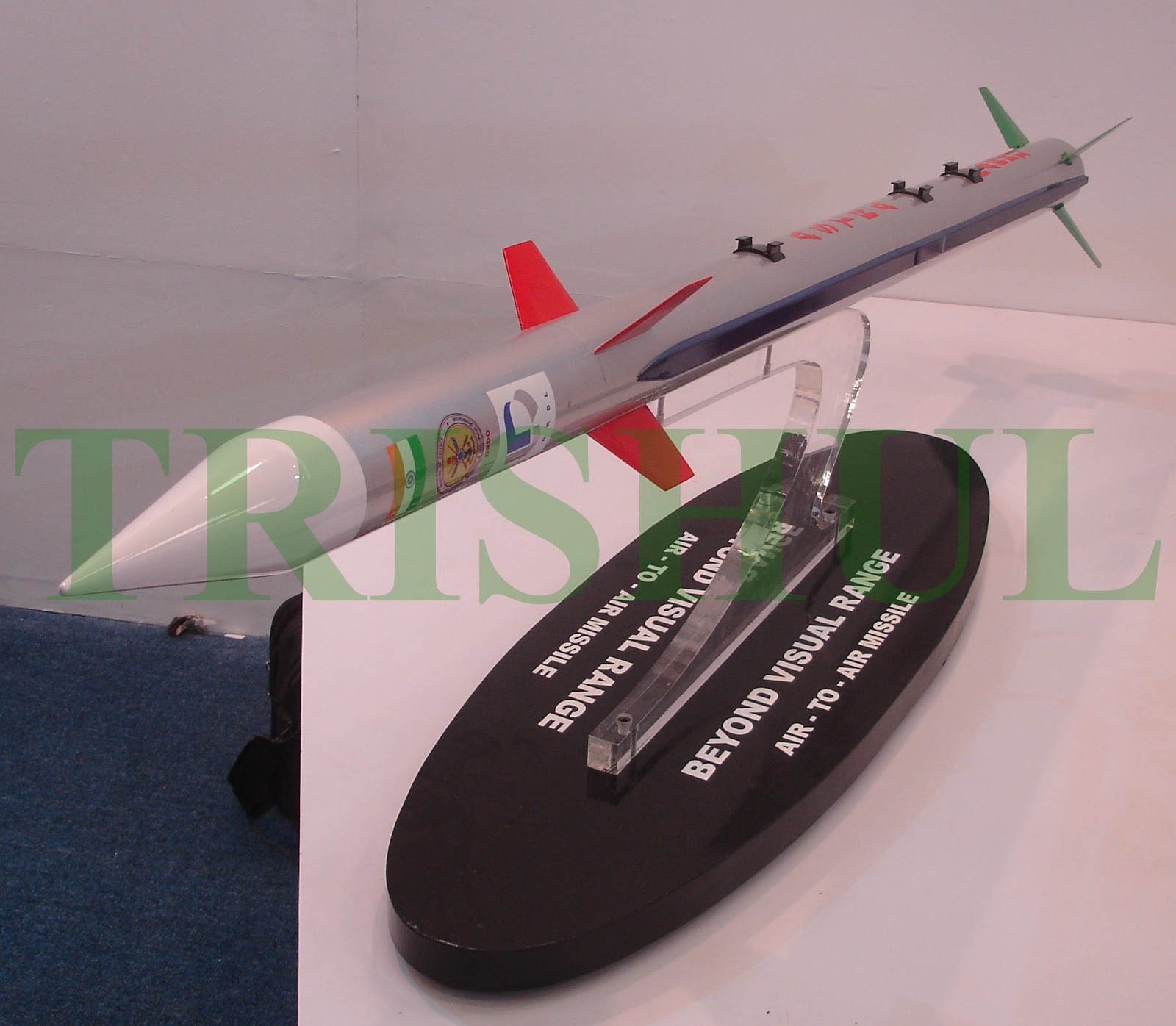
Aditya_V wrote:The image on page 5, it could well be a AAM, we dont from the scaled down model. Given it has 8 external control surfaces, AAM would be a very likely candidate, with the 1 stage pushing the missile to MAch 4+ and dropping off the 2nd stage igniting to give end game energy to the missile.
picture in the link posted above.https://www.iisc.ac.in/indias-first-e-m ... ransistor/
India’s first e-mode Gallium-Nitride Power Transistor
Why GaN HEMT?
All electronic devices that we use today have components made of semiconductors, mostly silicon. In recent years, gallium nitride (GaN), another semiconductor, is making its way into electronics as it is better suited for high power and high-frequency applications. Since GaN technology is still evolving, and it is less expensive to set up a foundry for manufacturing, it is touted to be India’s opportunity to mark its presence in the niche field of semiconductors. A interdisciplinary group of faculty members at IISc have developed India’s first-ever e-mode gallium nitride power transistor, whose performance is comparable to some of the best reports till date.
Power electronic systems that operate at high power and frequencies are projected to use specific transistors called High Electron Mobility Transistors or HEMTs. These transistors are made with gallium nitride, and they can operate at very high voltages, switch ON and OFF faster, and occupy less space when compared to silicon-based transistors. The projected market for HEMTs is projected to cross 5 Billion US$ and overall power device market is set to cross 18B$ mark by 2020, so one can say that GaN will acquire a major market share. With a growing market for electric vehicles in India, such an indigenous development to manufacture these transistors in India will save import costs and make us self-reliant for transistor technology.
What were the challenges with e-mode HEMT?
A High Electron Mobility Transistor (HEMT) has a conducting channel between two terminals, source and drain, and the current through the channel is controlled by a third terminal called gate. The HEMT channel is in a conducting state, or ON, unlike some of the other transistors, so current can pass through it as soon as it is powered on. To stop the flow of current, negative voltage needs to be applied at gate. However, for a transistor to operate reliably in power electronic circuits, it needs to be in the OFF state when no gate voltage is applied, which can then be turned ON by applying a voltage at the gate. Such operation is called e-mode or enhancement mode operation.
Commercially available transistors use various techniques to keep the transistor in normally OFF state One such approach is to completely recess the channel—which results in reducing the channel size. However, this affects the stability, performance and reliability of the device. Another approach is to use a gate made of gallium nitride, doped with impurities that deplete electrons from the channels and switch it OFF. The challenge with this method is that the gate and the channel form a diode, which starts conducting current when a voltage greater than a certain value is applied at the gate, making the unusable. Therefore, there was a need to build a new kind of e-mode HEMT, which is in the OFF state by default and works like any other commonly used transistor . Besides, it must be stable, reliable, efficient and can operate in the desired high voltage.
What is the New HEMT Technology Developed by IISc?
With the hardwork of two years paying off, the team at IISc were able to develop the first-ever e-mode gallium nitride power transistor from India that operates at 600V. It has many advantages in terms of performance and power handling capacity over similar devices proposed by other researchers, some of which are now in the market. Given that the 600V class e-mode HEMT technology recently got commercialised, IISc’s competition was with industry-standard state-of-the-art power gallium nitride HEMT technology. Keeping system level requirements in mind, this group has developed both e-mode HEMT as well as GaN Schottky diodes. Their work has been published in the IEEE Transactions on Electron Devices.
The researchers explored oxides of copper, nickel, aluminium and titanium for using them to make the gate of the improvised HEMT. They zeroed in on titanium oxide as it had minimal leakage current and provided better control of the voltage needed to turn the transistor ON. They finally used aluminium titanium oxide as the percentage of aluminium could be controlled during the fabrication process, which acts as a ‘control knob’, regulating the voltage needed to turn the transistor ON. Since aluminium titanium oxide is stable, it results in high reliability of the transistor.
Interestingly, the addition of aluminium in the titanium oxide was an accidental discovery! The team was experimenting with titanium oxide, trying to finetune it to achieve optimal characteristics. A particular lot that they had developed displayed characteristics totally inconsistent with, but better than, any previous lots. Investigation showed that there had been aluminium contamination, after which, the team explored the use of aluminium doping in titanium oxide.
The researchers carried out rigorous design of experiments, processed over 200 process lots to develop this technology and tested more than 150 transistors per manufacturing lot to develop the confidence with statistics. They found that the gallium nitride transistors with aluminium titanium oxide gate had a 100 fold reduction in the leakage current and better gate control, while keeping it under e-mode, as compared to other conventional GaN HEMTs. Besides, the current carrying capacity of the transistor when it is turned ON was found to be at par with industry standards.
Who Funded this Project?
This project has been funded by the Advanced Manufacturing Technology (AMT) initiative of Department of Science and Technology (DST), Govt. of India, with an initial support of 10.28 Crores. The key objective of DST’s AMT division, as far as this project is concerned, is to enable indigenous development of technologies, which are key to the nation’s economic and strategic growth. The GaN activity in IISc was seeded by the Ministry of Defence (MoD), which was subsequently supported by the Ministry of Electronics and Information Technology (MeitY) for the development of GaN based power electronics. These initiatives by MoD and MeitY on materials and devices have helped lay the platform for this advancement.
This is not any old story. Please read the linked article again. The team was actually funded by multiple GOI agencies and has developed a working item. Clearly, GOI did not want to commit to an expensive fab before being sure they had working tech. in place.Raghunathgb wrote:This is old story. The team even kept the proposal of developing a fab at the cost of 2500 crores which was rejected by central government in Dec 18. The team had a alternate plan to pursue this by taking a loan of 300 CR for this. However it seems to be moving towards dead end with no further encouragement coming by.
Meanwhile:“They (IISc) have prepared a detailed project report. It needs a different kind of appraisal —financial and sustainability and profitability. Everything has to be considered because fab you know is a very big project,” a Ministry of Electronics and Information Technology (Meity) official told ET. “The discussions are on between us, Niti aayog and the IISc team,” said the Meity official without specifying a timeline for the project approval. While India is taking initial steps with GaN semiconductor...
“There seems to be a huge barrier that semiconductor manufacturing cannot be done in India. I am pretty sure that perception existed before CeNSe (Centre for Nano Science and Engineering) came in. We showed that it can be done in India,” said Prof Srinivasan Raghavan, who leads the ten-member team from IISc for the project.
The team has gathered expertise from design of chips to building systems for applications. The two biggest applications are power electronics and RF electronics. In RF electronics, the two most common and visible applications, one would be military radar installations, wireless towers and cellphone towers for 5G. The ecosystem for GaN in terms of devices is there.
The IISc team has submitted two proposals: the first Rs 2,500 crore greenfield facility and managing it for five years. It includes design and roll out of a qualified product in 36 months. The second one is Rs 300 crore line in CeNSe facility and roll out of the first product in 24 months. “If we have to become leaders of this technology, the government has to fund it. That is the way they have done it in China, Taiwan and Korea. It has to be a government-funded and privately operated company,” The government is yet to finalise the funding mechanism, said the Meity official.
https://www.iitk.ac.in/new/data/Annual- ... 1-2018.pdfThe SPICE model titled ASM-THEMT has been selected as the world's first industry standard model for GalliumNitrideHighElectronMobilityTransistor (GaNHEMT)bySiliconIntegrationInitiative's CompactModelCoalition(CMC).TheIndustry standard models are selected after rigorous evaluation andvalidationofmultipletechnologiesbythe semiconductor industry. The model will now be available in Electronic Design Automation software, and will be used by major semiconductor and EDA companies worldwide. GaN HEMT is widely used in RF power amplifiers and power electronics applications. GaN HEMTs will be key to design power amplifiers for future 5G technology. The Government ofIndia is considering setting up a GaN foundry near Bengaluru. DRDOandISROarealsoactivelyworkingon developingthistechnologyfordefenseandspace applications.
QRSAM?Aditya_V wrote:The image on page 5, it could well be a AAM, we dont from the scaled down model. Given it has 8 external control surfaces, AAM would be a very likely candidate, with the 1 stage pushing the missile to MAch 4+ and dropping off the 2nd stage igniting to give end game energy to the missile.
welcome sir,,ramana wrote:Jaysimha Thanks for the Hindu report on the role of women engineers in Saras Program.

So was the composite material developed with Tata? Or Tata was just the manufacturer?jaysimha wrote:
some more from NAL website.
SUCCESSFUL COMMERCIALISATION OF COMPOSITE TECHNOLOGY
https://www.nal.res.in/en/latestupdate?ar_id=150
tata must have played a major role since Mr. CR SATHYA, FORMER GROUP DIRECTOR, VSSCchola wrote: So was the composite material developed with Tata? Or Tata was just the manufacturer?
